- 您现在的位置:买卖IC网 > Sheet目录1998 > ICS874001AGI-02LF (IDT, Integrated Device Technology Inc)IC PCI EXPRSS/JITT ATTEN 20TSSOP
ICS874001AGI-02 REVISION A AUGUST 30, 2010
13
2010 Integrated Device Technology, Inc.
ICS74001I-02 Data Sheet
PCI EXPRESS JITTER ATTENUATOR
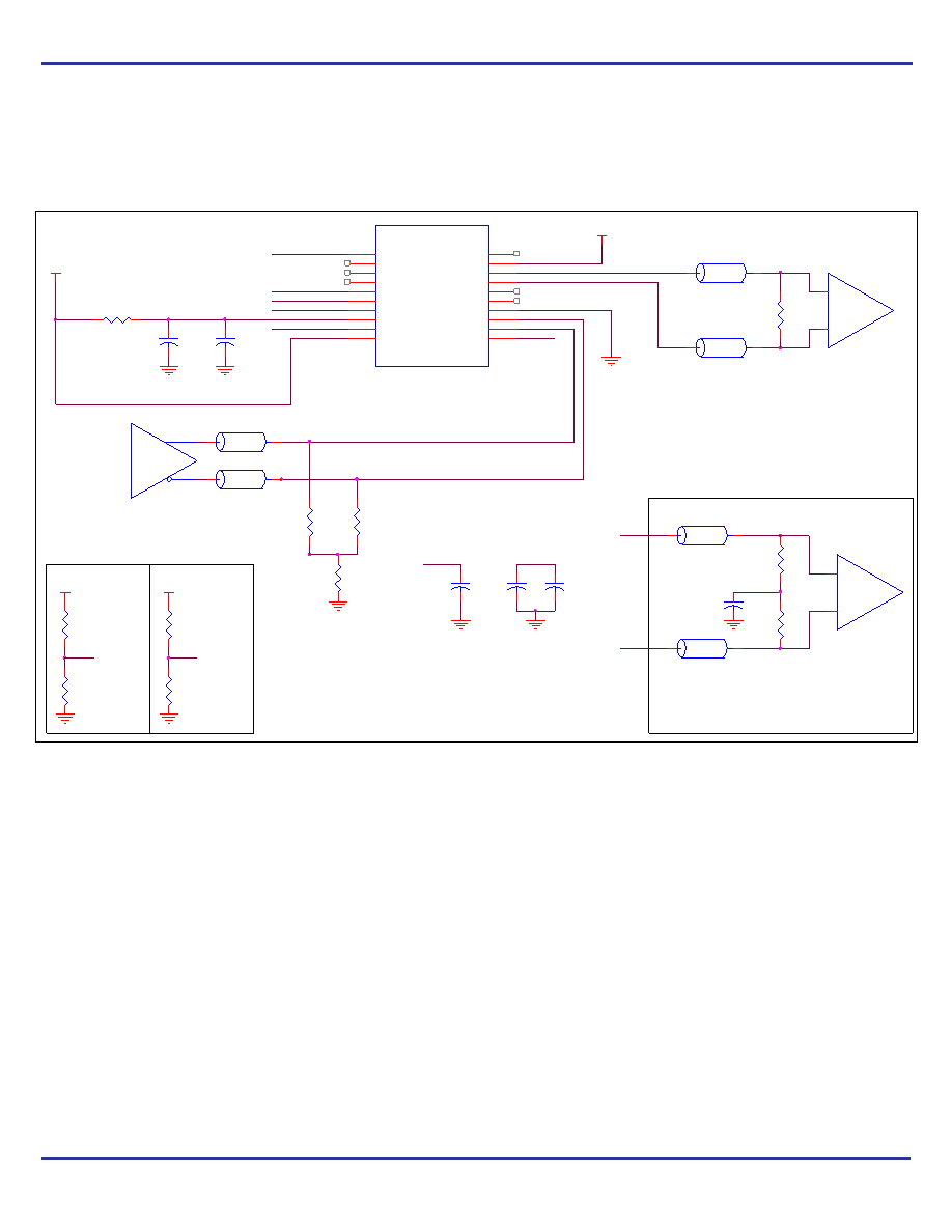
Schematic Layout
Figure 5 shows an example of ICS874001I-02 application
schematic. In this example, the device is operated at VDD =
3.3V. The decoupling capacitors should be located as close as
possible to the power pin. The input is driven by a 3.3V
LVPECL driver.
Figure 5. ICS874001I-02 Schematic Layout
VDD
VDDA
Zo = 50 Ohm
+
-
R4
50
nQ
(U1:19)
F_SEL1
(U1:10)
VDDO
VDD
PLL_SEL
Alternate
LVDS
Termination
GND
R1
100
+
-
RU2
Not Install
RU1
1K
RD2
1K
RD1
Not Install
Zo = 50 Ohm
VDD
nCLK
CLK
VDDO
nQ
VDDO = 3.3V
QQ
VDD = 3.3V
C7
.1uf
C6
10uf
nQ
Q
C5
.1uf
U1
nc
2
nc
3
nc
4
MR
5
BW_SEL
6
F_SEL1
7
VDDA
8
F_SEL0
9
VDD
10
OE
11
CLK
12
nCLK
13
GND
14
nc
15
nc
16
nQ
17
Q
18
VDDO
19
nc
20
PLL_SEL
1
R2
10
C2
10u
C1
0.1u
LVPECL Driv er
Zo = 50 Ohm
R8
50
R7
50
R6
50
MR
BW_SEL
F_SEL0
OE
To Logic
Input
pins
Set Logic
Input to
'1'
Logic Control Input Examples
Set Logic
Input to
'0'
To Logic
Input
pins
R5
50
C3
0.1uF
发布紧急采购,3分钟左右您将得到回复。
相关PDF资料
ICS874001AGI-05LFT
IC PCI EXPRSS/JITT ATTEN 20TSSOP
ICS874002AGLFT
IC PCI EXPRSS/JITT ATTEN 20TSSOP
ICS874005AG-04LFT
IC PCI EXPRSS/JITT ATTEN 24TSSOP
ICS874005AGLFT
IC PCI EXPRSS/JITT ATTEN 24TSSOP
ICS8741004AGLFT
IC PCI EXPRSS/JITT ATTEN 24TSSOP
ICS87604AGILF
IC CLK MULT/ZD BUFFER 28-TSSOP
ICS8761CYLFT
IC CLK GEN PCI/PCI-X 64-LQFP
ICS87946AYILFT
IC CLOCK GENERATOR 32-LQFP
相关代理商/技术参数
ICS874001AGI-02LFT
功能描述:IC PCI EXPRSS/JITT ATTEN 20TSSOP RoHS:是 类别:集成电路 (IC) >> 时钟/计时 - 专用 系列:FemtoClock™, PCI Express™ (PCIe) 标准包装:1,500 系列:- 类型:时钟缓冲器/驱动器 PLL:是 主要目的:- 输入:- 输出:- 电路数:- 比率 - 输入:输出:- 差分 - 输入:输出:- 频率 - 最大:- 电源电压:3.3V 工作温度:0°C ~ 70°C 安装类型:表面贴装 封装/外壳:28-SSOP(0.209",5.30mm 宽) 供应商设备封装:28-SSOP 包装:带卷 (TR) 其它名称:93786AFT
ICS874001AGI-05LF
功能描述:IC PCI EXPRSS/JITT ATTEN 20TSSOP RoHS:是 类别:集成电路 (IC) >> 时钟/计时 - 专用 系列:FemtoClock™, PCI Express™ (PCIe) 标准包装:1 系列:- 类型:时钟/频率发生器,多路复用器 PLL:是 主要目的:存储器,RDRAM 输入:晶体 输出:LVCMOS 电路数:1 比率 - 输入:输出:1:2 差分 - 输入:输出:无/是 频率 - 最大:400MHz 电源电压:3 V ~ 3.6 V 工作温度:0°C ~ 85°C 安装类型:表面贴装 封装/外壳:16-TSSOP(0.173",4.40mm 宽) 供应商设备封装:16-TSSOP 包装:Digi-Reel® 其它名称:296-6719-6
ICS874001AGI-05LFT
功能描述:IC PCI EXPRSS/JITT ATTEN 20TSSOP RoHS:是 类别:集成电路 (IC) >> 时钟/计时 - 专用 系列:FemtoClock™, PCI Express™ (PCIe) 标准包装:1,500 系列:- 类型:时钟缓冲器/驱动器 PLL:是 主要目的:- 输入:- 输出:- 电路数:- 比率 - 输入:输出:- 差分 - 输入:输出:- 频率 - 最大:- 电源电压:3.3V 工作温度:0°C ~ 70°C 安装类型:表面贴装 封装/外壳:28-SSOP(0.209",5.30mm 宽) 供应商设备封装:28-SSOP 包装:带卷 (TR) 其它名称:93786AFT
ICS874002AGLF
功能描述:IC JITTER ATTENUATOR 20-TSSOP RoHS:是 类别:集成电路 (IC) >> 时钟/计时 - 专用 系列:HiPerClockS™, PCI Express® (PCIe) 标准包装:1 系列:- 类型:时钟/频率发生器,多路复用器 PLL:是 主要目的:存储器,RDRAM 输入:晶体 输出:LVCMOS 电路数:1 比率 - 输入:输出:1:2 差分 - 输入:输出:无/是 频率 - 最大:400MHz 电源电压:3 V ~ 3.6 V 工作温度:0°C ~ 85°C 安装类型:表面贴装 封装/外壳:16-TSSOP(0.173",4.40mm 宽) 供应商设备封装:16-TSSOP 包装:Digi-Reel® 其它名称:296-6719-6
ICS874002AGLFT
功能描述:IC PCI EXPRSS/JITT ATTEN 20TSSOP RoHS:是 类别:集成电路 (IC) >> 时钟/计时 - 专用 系列:HiPerClockS™, PCI Express® (PCIe) 标准包装:1,500 系列:- 类型:时钟缓冲器/驱动器 PLL:是 主要目的:- 输入:- 输出:- 电路数:- 比率 - 输入:输出:- 差分 - 输入:输出:- 频率 - 最大:- 电源电压:3.3V 工作温度:0°C ~ 70°C 安装类型:表面贴装 封装/外壳:28-SSOP(0.209",5.30mm 宽) 供应商设备封装:28-SSOP 包装:带卷 (TR) 其它名称:93786AFT
ICS874003AG-02LF
功能描述:IC JITTER ATTENUATOR 20-TSSOP RoHS:是 类别:集成电路 (IC) >> 时钟/计时 - 专用 系列:HiPerClockS™, FemtoClock™, PCI Express® (PCIe) 标准包装:1 系列:- 类型:时钟/频率发生器,多路复用器 PLL:是 主要目的:存储器,RDRAM 输入:晶体 输出:LVCMOS 电路数:1 比率 - 输入:输出:1:2 差分 - 输入:输出:无/是 频率 - 最大:400MHz 电源电压:3 V ~ 3.6 V 工作温度:0°C ~ 85°C 安装类型:表面贴装 封装/外壳:16-TSSOP(0.173",4.40mm 宽) 供应商设备封装:16-TSSOP 包装:Digi-Reel® 其它名称:296-6719-6
ICS874003AG-02LFT
功能描述:IC PCI EXPRSS/JITT ATTEN 20TSSOP RoHS:是 类别:集成电路 (IC) >> 时钟/计时 - 专用 系列:HiPerClockS™, FemtoClock™, PCI Express® (PCIe) 标准包装:1,500 系列:- 类型:时钟缓冲器/驱动器 PLL:是 主要目的:- 输入:- 输出:- 电路数:- 比率 - 输入:输出:- 差分 - 输入:输出:- 频率 - 最大:- 电源电压:3.3V 工作温度:0°C ~ 70°C 安装类型:表面贴装 封装/外壳:28-SSOP(0.209",5.30mm 宽) 供应商设备封装:28-SSOP 包装:带卷 (TR) 其它名称:93786AFT
ICS874003AG-04LF
功能描述:IC PCI EXPRSS/JITT ATTEN 20TSSOP RoHS:是 类别:集成电路 (IC) >> 时钟/计时 - 专用 系列:HiPerClockS™, FemtoClock™, PCI Express® (PCIe) 标准包装:1,500 系列:- 类型:时钟缓冲器/驱动器 PLL:是 主要目的:- 输入:- 输出:- 电路数:- 比率 - 输入:输出:- 差分 - 输入:输出:- 频率 - 最大:- 电源电压:3.3V 工作温度:0°C ~ 70°C 安装类型:表面贴装 封装/外壳:28-SSOP(0.209",5.30mm 宽) 供应商设备封装:28-SSOP 包装:带卷 (TR) 其它名称:93786AFT